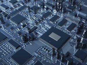
Silicon chips are a key component of all electronic devices around the world. They essentially act like a brain, computing, processing information, controlling and storing data. They are most commonly associated with CPUs, GPUs, RAM and other computer components, but their range of applications is much broader. In general, chips are the basis of modern electronics that have revolutionized our world.
The entire technology is based on the semiconductor material silicon, which means that it can be a conductor as well as an insulator depending on its state. This is the substrate to start the semiconductor manufacturing process.
The intricate process of chip fabrication consists of several basic steps and requires a lot of sophisticated machinery and very strict environmental conditions, so semiconductor equipment manufacturers have a very challenging mission to meet all the requirements.
Wafer fabrication
The process begins with the extraction of raw silicon from sand, which is turned into a high-purity liquid when heated. With the addition of carbon and special processing, it is possible to receive a bar of silicon crystal, called an ingot. It is then cut into very thin discs called wafers, each of which is polished mechanically and chemically. The surface must be spotless and smooth, as any defects have a negative effect on the final product. A wafer prepared in this way does not yet conduct electricity, so subsequent processes bring in semiconductivity.
Deposition
It is the creation of thin films of silicon oxide, aluminum or other metals on the polished surface of a wafer. Depending on the type of product to be fabricated, the deposited material should provide insulation, conduction or semiconduction.
Now, after another cleaning, prefabrication is complete and the crucial phase – photolithography and etching – can begin.
Photolithography
First, start by coating with photoresist – a material that reacts to light. A very thin layer is applied on top of the deposited thin film. To create a uniform layer, a centrifugal method is used, and the device used is a spin-coater.
Now the wafers are treated with light transmitted through a photomask with the desired pattern to draw the circuits on the surface. The photoresist material in the designed areas is exposed to the light, which removes it and exposes a thin film from the previous process, and the remaining material will act as a mask for the next step.
Etching
The wafer is then treated with a gas or liquid etchant, which is responsible for selectively removing the deposited thin film from the substrate in uncovered areas.
These two semiconductor chip manufacturing processes – photolithography and etching – are repeated several times and create dozens of layers to deliver the desirable complex 3D architecture.
Ion Implantation
This operation gives the exposed areas of the wafer semiconductor properties. Impurity atoms are implanted into the substrate and change the conductivity due to the specific atomic structure of silicon.
Then, after heat activation, micro-transistors are successfully created.
Metallization
Electrical contacts must be connected in specific, engineered layouts. Interconnections on the wafer are first made by depositing metal alloys in sputtering machines, and then etched to ensure the proper architecture. The chip is almost ready!
Quality control and packaging
Now is the time for testing, quality control for reliability and defect detection. Once completed, to produce individual chips, they are separated by cutting called dicing.
Then we can finally mount the semiconductor chip in the electronic device and connect. Conventional methods or innovative additive technologies can be used for this purpose. XTPL S.A. has developed a dispensing technology for interconnections powered by conductive nano-inks. The ultra-precise structures can be printed directly onto chips and other components to connect inputs and outputs, and function like wires, but printed!
Conclusion
The semiconductor chip manufacturing process is a marvel of micro-engineering, pushing the boundaries of precision and miniaturization. From the raw silicon material to the brains of our advanced devices, every chip goes through a complex process of fabrication and testing. The microelectronics industry is constantly innovating and uncovering more remarkable developments to shape the future of electronic devices and digital world.